
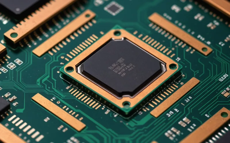
The package does not show up in the RF simulation. It shows up in the measurement when the device fails to reproduce the simulated performance. At Ka-band, from 26.5 to 40 GHz, parasitics that are negligible at X-band become the dominant source of degraded gain, shifted matching, and elevated thermal resistance. Choosing a package type early and treating it as a variable to co-optimize with the die is not a luxury for Ka-band PA development; it is a requirement.
Three package architectures dominate in production-grade Ka-band PA modules: QFN (quad flat no-lead), laminate-based multi-chip modules, and bare-die attach. Each imposes a different set of tradeoffs across three axes that matter for phased-array satcom and 5G mmWave front-ends: parasitic inductance and its effect on impedance matching, thermal resistance from junction to board, and assembly yield in high-volume surface-mount processes.
QFN: The First Choice That Gets Questioned at Frequency
QFN packaging has become ubiquitous in RF semiconductors at frequencies through C-band and into X-band. The exposed thermal pad reduces junction-to-board resistance compared to gull-wing lead frames. Eliminating bond wires via wafer-level or flip-chip attachment reduces parasitic inductance substantially. A properly designed QFN with a solder-attach thermal pad and flip-chip die mount can achieve junction-to-board thermal resistance below 15 degrees per watt for a 5x5 mm footprint device.
At 28 to 40 GHz, though, the QFN encounters two challenges. First, the lead frame metal at the package periphery creates ground inductance that varies with the number and placement of the exposed pads connected to the system board. Ground inductance in a Ka-band PA's source terminal directly degrades gain and complicates input matching. The typical QFN design response is to connect many peripheral pads to ground and rely on via stitching in the system board to minimize the inductance to the RF ground plane. Done carefully, this works. Done carelessly, the printed circuit board absorbs more Ka-band signal than the PA die.
Second, the QFN lid or overmold adds dielectric boundary conditions that affect impedance inside the package. Encapsulant permittivity interacts with the internal bond wire geometry or RDL traces. Some QFN variants use a ceramic cap over a metal carrier, which is dimensionally stable but adds cost and constrains the internal routing geometry. For a standard commercial Ka-band PA operating between 26.5 and 30 GHz, QFN is a viable first choice. For a device required to maintain consistent gain and match from 26.5 to 40 GHz, the package resonances and parasitic sensitivities that QFN imposes often force a switch to a different platform.
Laminate Multi-Chip Modules: Integration at the Cost of Complexity
A laminate MCM uses a multi-layer organic substrate, typically constructed on a PTFE-based or modified FR4 microwave laminate, to interconnect multiple dice: PA die, driver stage, output impedance matching network, and bias decoupling capacitors. The package boundary is often not the functional RF boundary; the matching network is inside the module, so the part number delivered to the system integrator is a pre-matched, pre-biased amplifier with standardized RF ports.
This pre-matching architecture significantly simplifies system-level RF integration. The external board no longer needs to implement Ka-band matching networks for the bare PA die. That means fewer board layers, fewer critical microwave tuning iterations, and simpler assembly process at the radio unit level. For a hardware team integrating 32 or 64 PA elements in a phased array, multiplying complex matching network tuning across every element position is a serious development bottleneck. The MCM approach shifts that complexity to the module supplier and leaves a well-characterized matched module as the integration primitive.
The tradeoffs are real. Laminate MCM thermal resistance is generally higher than QFN because heat must conduct through the laminate substrate to reach the board. For a PA dissipating 4 to 6 W per element, the laminate's thermal conductivity, typically 0.2 to 0.5 W/m.K for PTFE-based materials versus 3 W/m.K for aluminum nitride ceramic, creates a junction temperature differential of 20 to 40 degrees above ambient for a given cooling solution. That thermal hit must be accounted for in the power and reliability budget. If the system runs the PA at less than full rated power to stay within junction temperature, the efficiency advantage of a high-P1dB GaN device partially erodes.
MCM assembly yield also depends on the die attach process quality. Voids in the die attach epoxy or solder paste under the die increase thermal resistance and degrade reliability at field temperatures. X-ray inspection of the attach quality is a standard process step in Ka-band MCM production for satellite and defense applications.
Bare-Die Attach: Control and Constraints
Bare-die attach, placing an unpackaged die directly on the system substrate or on a custom metal carrier, gives the RF designer maximum control over the impedance environment at the die. There is no package ground inductance, no lid dielectric, and no encapsulant interacting with the RF field. The die's output pads can be connected by carefully length-controlled bond wires or via controlled-collapse flip-chip bumps directly to the system-level matching network on the RF module substrate.
Thermal resistance with bare die on a copper-molybdenum or aluminum nitride carrier is the lowest achievable in any of these package options, routinely achieving junction-to-carrier values below 10 degrees per watt for a well-attached GaN die. This is why bare-die configurations are common in military and space applications where thermal management is design-critical and assembly cost is secondary to performance.
The constraint is assembly. Bare-die attach requires cleanroom handling, trained bond wire or flip-chip assembly operators, and a volume of post-assembly RF test and calibration that offsets the raw performance gain. Wire bond reproducibility at Ka-band introduces unit-to-unit gain and phase variation that must be tracked and compensated in phased-array calibration. For a production run of 10,000 array elements, bare-die assembly cost and calibration overhead is a genuine economic constraint, not a theoretical one.
Parasitic Inductance: The Number That Governs the Choice
A useful engineering frame: the source inductance that a packaging choice imposes determines the self-feedback at Ka-band. Source inductance of 0.1 nH at 35 GHz presents a reactive impedance of approximately 22 ohms. For a GaN device with 50 ohm source termination, that corresponds to significant negative feedback that reduces gain and shifts the input reflection. Going from 0.3 nH to 0.05 nH source inductance can recover 1 to 2 dB of gain at 35 GHz without changing the die at all.
QFN with flip-chip die mount achieves 0.05 to 0.15 nH depending on configuration. A bond wire connection to an exposed pad in a QFN adds 0.3 to 0.8 nH per bond wire. Laminate MCM with buried microstrip via connections achieves 0.05 to 0.1 nH on a high-quality microwave laminate but the external RF transition adds its own parasitic. Bare-die with careful RF substrate design can achieve the lowest values, but only if the substrate's own parasitic environment is controlled.
We are not suggesting that QFN is wrong for Ka-band applications, or that bare die is always the right choice. The package type that is correct depends on whether system-level RF integration complexity, thermal management, or production yield is the binding constraint for a given program. An active antenna unit for a phased array satcom terminal with 48 elements has a different optimization landscape than a ground-based radar module where the die count is low and the thermal budget is generous. The FA-2400 series is currently being specified with QFN and laminate MCM variants because both integration scenarios are real for the applications we are targeting, and the design target thermal resistance is achievable in either packaging approach if the board-level implementation is correct.
Ka-Band Assembly Rules Worth Enforcing
Regardless of package type, several assembly and layout rules consistently distinguish working Ka-band PA modules from modules that require multiple PCB spins to achieve datasheet performance. Ground via spacing below the package must be below lambda/8 at the highest frequency of interest to maintain a low-inductance RF ground. This translates to via pitch below 0.9 mm at 40 GHz. Solder paste volume under QFN thermal pads must be tightly controlled; a void area above 25% of the pad area visibly increases thermal resistance and can cause field failures under thermal cycling.
Microstrip transitions from the package RF ports to the board transmission line must be modeled, not estimated. A connector or via transition that works well at 18 GHz may present a standing wave at 38 GHz that degrades the PA's load impedance enough to affect gain flatness. Pre-layout electromagnetic simulation of the package-to-board transition is not over-engineering for Ka-band work; it is the difference between a first-spin PCB that works and one that has a 3 dB gain anomaly at mid-band that requires another tape-out to trace to the transition.